Introduction#
lib_sw_pll provides software that, together with the xcore.ai application PLL, provides a PLL
that will generate a clock that is phase-locked to an input clock.
lib_sw_pll is intended to be used with the XCommon CMake
, the XMOS application build and dependency management system.
How the Software PLL works#
PLLs#
A Phase Locked Loop (PLL) is a normally dedicated hardware that allows generation of a clock which is synchronised to an input reference clock by both phase and frequency. They consist of a number of sub-components:
A Phase Frequency Detector (PFD) which measures the difference (error) between a reference clock and the divided generated clock.
A control loop, typically a Proportional Integral (PI) controller to close the loop and zero the error.
A Digitally Controlled Oscillator (DCO) which converts a control signal into a clock frequency.
fig_basic_block depicts a block diagram of a basic PLL.
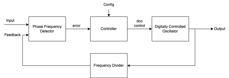
Basic PLL Block Diagram#
xcore.ai devices have on-chip a secondary PLL sometimes known as the Application PLL. This PLL multiplies the clock from the on-board crystal source and has a fractional register allowing very fine control over the multiplication and division ratios from software.
However, it does not support an external reference clock input and so cannot natively track and lock to an external clock reference. This software PLL module provides a set of scripts and firmware which enables the provision of an input reference clock which, along with a control loop, allows tracking of the external reference over a certain range. It also provides a lower level API to allow tracking of virtual clocks rather than physical signals such as when receiving digital samples from another device or packets over a network.
There are two types of PLL, or specifically Digitally Controlled Oscillators (DCO), supported in
this library; Look-up Table (LUT) and Sigma-delta Modulator (SDM).
There are trade-offs between the two types of DCO, which are summarised in table_lut_vs_dco.
Comparison item |
LUT DCO |
SDM DCO |
|---|---|---|
Jitter |
Low, 1-2 ns |
Very Low, 10-50 ps |
Memory Usage |
Low, ~2.5 kB |
Low, ~2 kB |
MIPS Usage |
Low - ~1 |
High - ~50 |
Lock Range PPM |
Moderate, 100-1000 |
Wide, 1500-3000 |
Note
Jitter is measured using a frequency mask of 100 Hz to 40 kHz as specified by AES-12id-2006.
A fixed (non phase-locked) PLL setup API is also available which assumes a 24 MHz XTAL frequency and provides output frequencies of 11.2896 MHz, 12.288 MHz, 22.5792 MHz, 24.576 MHz, 45.1584 MHz or 49.152 MHz. Output jitter for fixed clocks using a 100 Hz to 40 kHz mask is typically less than 8 ps. See the Common API section.
LUT based DCO#
The LUT based DCO allows a discrete set of fractional settings resulting in a fixed number of frequency steps.
The LUT is pre-computed table which provides a set of monotonically increasing frequency register settings. The LUT
based DCO requires very low compute allowing it to be run in a sample-based loop at audio
frequencies such as 48kHz or 44.1kHz. It required two bytes per LUT entry and provides reasonable
jitter performance suitable for voice or entry level Hi-Fi. fig_lut_pll depicts a LUT DCO
based PLL
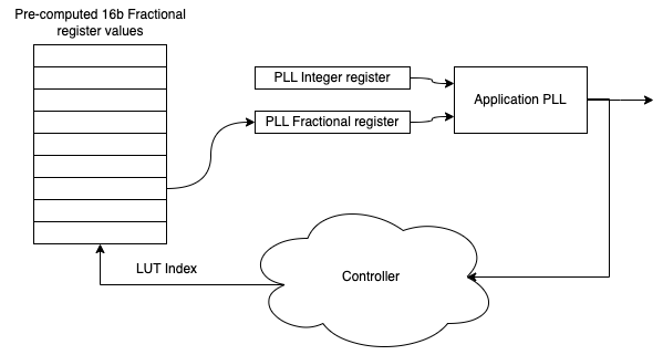
LUT DCO based PLL#
The range is governed by the look up table (LUT) which has a finite number of entries and consequently
has a frequency step size. This affects the output jitter performance when the controller oscillates between two
settings once locked. Note that the actual range and number of steps is highly configurable.
fig_lut_dco_range shows an example of LUT discrete output frequencies.
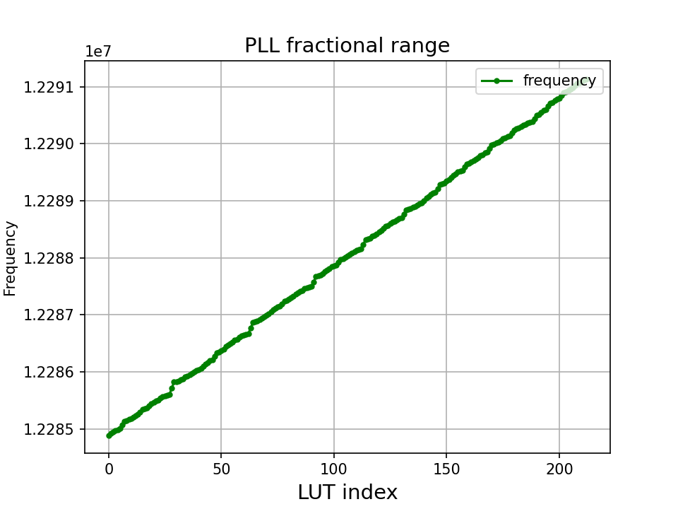
Example of LUT discrete output frequencies#
The index into the LUT is controlled by a PI controller which multiplies the error input and integral error input by the supplied loop constants. An integrated wind up limiter for the integral term is nominally set at 2x the maximum LUT index deviation to prevent excessive overshoot where the starting input error is high. A double integrator term is also available to help zero phase error.
fig_tracking_lut shows a time domain plot of how the controller (typically running at
around 100 Hz) selects between adjacent LUT entries. fig_modulated_fft_lut shows the
consequential frequency modulation effect.
LUT selection when tracking a constant input frequency#

LUT noise plot when when tracking a constant input frequency#
SDM Based DCO#
The SDM based DCO provides a fixed number (9 in this case) of frequency steps which are jumped between at a high rate (eg. 1 MHz) but requires a dedicated logical core to run the SDM algorithm and update the PLL fractional register. The SDM is third order.
The SDM typically provides better audio quality by pushing the noise floor up into the
inaudible part of the spectrum. A fixed set of SDM coefficients and loop filters are provided which
have been hand tuned to provide either 24.576 MHz or 22.5792 MHz low jitter clocks and are suitable for Hi-Fi
and professional audio applications. fig_sdm_pll depicts a SDM DCO based PLL.
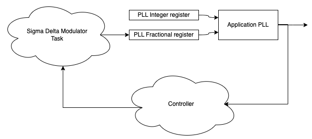
SDM DCO based PLL#
The steps for the SDM output are quite large which means a wide range is typically available.
fig_sdm_dco_range shows SDM discrete output frequencies.
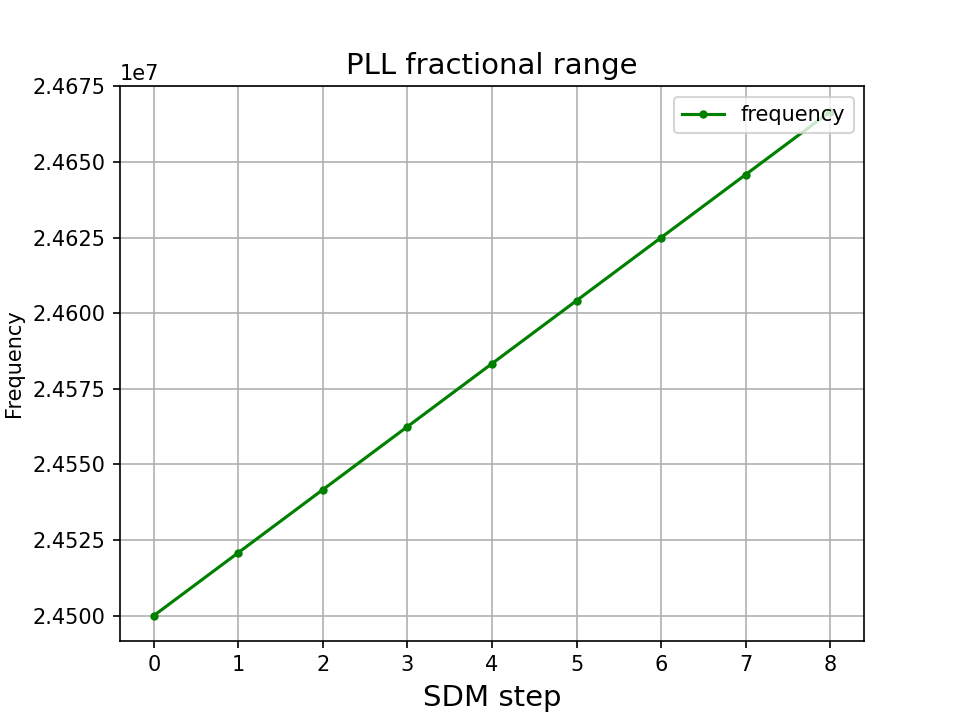
SDM discrete output frequencies#
fig_sdm_tracking shows a time domain plot of how the Sigma Delta Modulator jumps rapidly
between multiple frequencies. fig_modulated_fft_sdm shows the consequential spread of the
noise floor.
SDM frequency selection when tracking a constant input frequency#
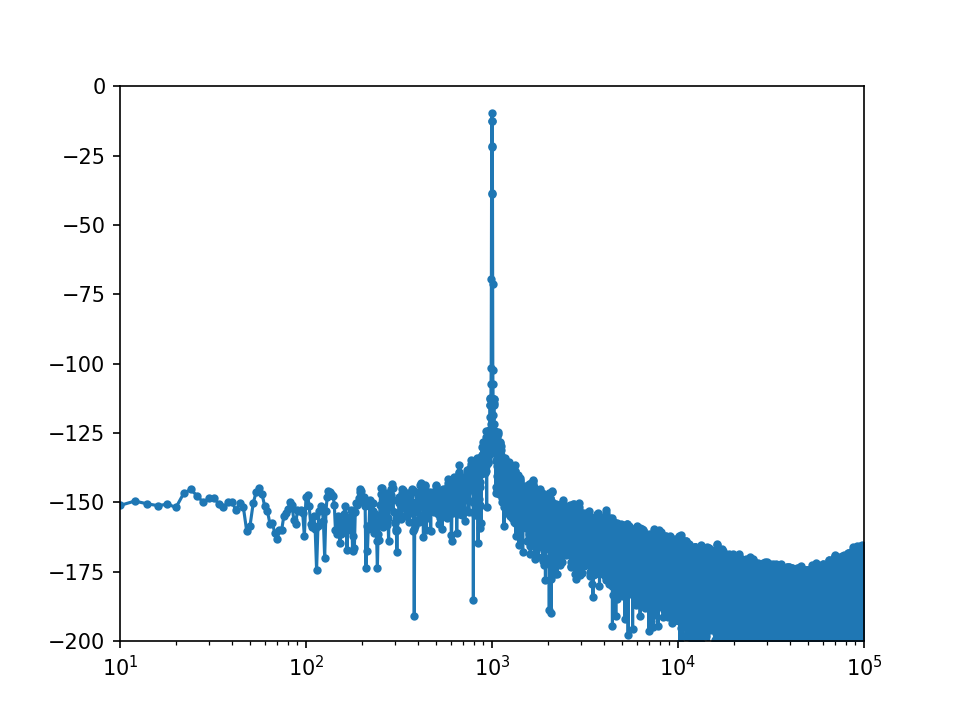
SDM noise plot when when tracking a constant input frequency#
Phase Frequency Detector#
The Software PLL Phase Frequency Detector (PFD) detects frequency by counting clocks over a specific time period. The clock counted is the output from the PLL and the time period over which the count happens is a multiple of the input reference clock. This way the frequency difference between the input and output clock can be directly measured by comparing the read count increment with the expected count increment for the nominal case where the input and output are locked.
The PFD cannot directly measure phase, however, by taking the time integral of the frequency we can derive the phase which can be done by the PI controller.
The PFD uses three chip resources:
A one bit port to capture the PLL output clock (always Port 1D on Tile[1] of xcore.ai)
A clock block to turn the captured PLL output clock into a signal which can be distributed across the xcore tile
An input port (either one already in use or an unconnected dummy port such as Port 32A) clocked from the above clock block. The in-built counter of this port can then be read and provides a count of the PLL output clock.
Two diagrams showing practical xcore resource setups are shown in the Example application resource setup section.
The port timers are 16 bits and so the PFD must account for wrapping because the overflow period at, for example, 24.576 MHz is 2.67 milliseconds and a typical control period is in the order 10 milliseconds.
There may be cases where the port timer sampling time cannot be guaranteed to be fully isochronous, such as when a significant number of
instructions exist between a hardware event occur between the reference clock transition and the port timer sampling. In these cases
an optional input jitter reduction scheme is provided to allow scaling of the read port timer value. This scheme is used in the i2s_slave_lut
example where the port timer read is precisely delayed until the transition of the next BCLK which removes the instruction timing jitter
that would otherwise be present. The cost is 1/64th of LR clock time of lost processing in the I²S callbacks but the benefit is the jitter
caused by variable instruction timing to be eliminated.
Proportional Integral Controller#
The PI controller uses fixed point (15Q16) types and 64 bit intermediate terms to calculate the error and accumulated error which are summed to produce the output. In addition a double integral term is included to allow calculation of the integral term of phase error, which itself is the integral of the frequency error which is the output from the PFD.
Wind-up protection is included in the PI controller which clips the integral and double integral accumulator terms and is nominally set to LUT size for the LUT based DCO and the control range for the SDM based DCO.
The SDM controller also includes a low-pass filter for additional error input jitter reduction.
See the Tuning the Software PLL section for information about how to optimise the PI controller.
Simulation Model#
A complete model of the Software PLL is provided and is written in Python version 3.
Contents#
In the python/sw_pll directory you will find multiple files:
.
├── analysis_tools.py
├── app_pll_model.py
├── controller_model.py
├── dco_model.py
├── pfd_model.py
├── pll_calc.py
└── sw_pll_sim.py
These are all installable as a Python PIP module by running pip install -e . from the root of the repo.
Typically you do not need to access any file other than sw_pll_sim.py which brings in the other files as modules when run.
sw_pll_sim.py may be run with the argument LUT or SDM depending on which type of PLL you wish to simulate.
analysis_tools.py contains audio analysis tools for assessing the frequency modulation of a tone from the jitter in
the recovered clock.
controller_model.py models the PI controllers used in the Software PLL system.
dco_model.py contains a model of the LUT and SDM digitally controlled oscillators.
pfd_model.py models the Phase Frequency Detector which is used when inputting a reference clock to the Software PLL.
app_pll_model.py models the Application PLL hardware and allows reading/writing include files suitable for inclusion into xcore
firmware projects.
pll_calc.py is the command line script that generates the LUT. It is quite a complex to use script which requires in depth
knowledge of the operation of the App PLL. Instead it is recommended to use app_pll_model.py which calls pll_calc.py which
wraps the script with sensible defaults, or better, use one of the provided profiles driven by sw_pll_sim.py.
Running the PI simulation and LUT generation script#
By running sw_pll_sim.py LUT a number of operations will take place:
The
fractions.hLUT include file will be generated (LUT PLL only - this is not needed by SDM)The
register_setup.hPLL configuration file will be generated for inclusion in your xcore project.A graphical view of the LUT settings showing index vs. output frequency is generated.
A time domain simulation of the PI loop showing the response to steps and out of range reference inputs is run.
A wave file containing a 1 kHz modulated tone for offline analysis.
A log FFT plot of the 1 kHz tone to see how the PLL frequency steps affect a pure tone.
A summary report of the PLL range is also printed to the console.
The directory listing following running of sw_pll_sim.py will be added to as follows:
.
├── fractions.h
├── register_setup.h
├── tracking_lut.png
├── tracking_sdm.png
├── modulated_tone_1000Hz_lut.wav
├── modulated_tone_1000Hz_sdm.wav
├── modulated_fft_lut.png
└── modulated_fft_sdm.png
fig_pll_step_response shows the step response of the control loop when the target
frequency is changed during the simulation.
You can see it track smaller step changes but for the larger steps it can be seen to clip and not
reach the input step, which is larger than the used LUT size will allow. The LUT size can be
increased if needed to accommodate a wider range.
The step response is quite fast and you can see even a very sharp change in frequency is accommodated in just a handful of control loop iterations.
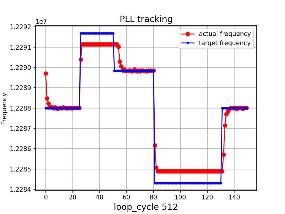
PLL step response#
Tuning the Software PLL#
LUT based PLL Tuning#
PI controller#
Typically the PID loop tuning should start with 0 Kp term and a small (e.g. 1.0) Ki term.
Decreasing the ref_to_loop_call_rate parameter will cause the control loop to execute more frequently and larger constants will be needed.
Try tuning Ki value until the desired response curve (settling time, overshoot etc.) is achieved in the
tracking_xxx.pngoutput.Kp can normally remain zero, but you may wish to add a small value to improve step response
Note
After changing the configuration, ensure you delete fractions.h otherwise the script will re-use the last calculated values. This is done to speed execution time of the script by avoiding the generation step.
A double integral term is supported in the PI loop because the clock counting PFD included measures the frequency error. The phase error is the integral of the frequency error and hence if phase locking is required as well as frequency locking then we need to support the integral of the integral of the frequency error. Changing the Kp, Ki and Kii constants and observing the simulated (or hardware response) to a reference change is all that is needed in this case.
Note
In the python simulation file sw_pll_sim.py, the PI constants Kp, Ki and optionally Kii can be found in the functions run_lut_sw_pll_sim() and run_sd_sw_pll_sim().
Typically a small Kii term is used, if needed, because it accumulates very quickly.
LUT example configurations#
The LUT implementation requires an offline generation stage which has many possibilities for customisation.
A number of example configurations, which demonstrate the effect on PPM, step size etc. of changing various parameters, is provided in the sw_pll_sim.py file.
Search for profiles and profile_choice in this file. Change profile choice index to select the different example profiles and run the python file again.
Output frequency MHz |
Reference frequency kHz |
Range +/- PPM |
Average step size Hz |
LUT size bytes |
|---|---|---|---|---|
12.288 |
48.0 |
250 |
29.3 |
426 |
12.288 |
48.0 |
500 |
30.4 |
826 |
12.288 |
48.0 |
1000 |
31.0 |
1580 |
24.576 |
48.0 |
500 |
60.8 |
826 |
24.576 |
48.0 |
100 |
9.5 |
1050 |
6.144 |
16.0 |
150 |
30.2 |
166 |
Note
The physical PLL actually multiplies the input crystal, not the reference input clock. It is the PFD and software control loop that detects the frequency error and controls the fractional register to make the PLL track the input. A change in the reference input clock parameter only affects the control loop and its associated constants such as how often the PI controller is called.
Custom LUT Generation Guidance#
The fractions lookup table is a trade-off between PPM range and frequency step size. Frequency step size will affect jitter amplitude as it is the amount that the PLL will change frequency when it needs to adjust. Typically, the locked control loop will slowly oscillate between two values that straddle the target frequency, depending on input frequency.
Small discontinuities in the LUT may be experienced in certain ranges, particularly close to 0.5 fractional values, so it is preferable
to keep in the lower or upper half of the fractional range. However the LUT table is always monotonic
and so control instability will not occur for that reason. The range of the LUT Software PLL can be seen
in the lut_dco_range.png image. It should be a reasonably linear response without significant
discontinuities. If discontinuities are seen, try moving the range towards 0.0 or 1.0 where fewer discontinuities may
be observed due the step in the fractions.
Steps to vary the LUT PPM range and frequency step size#
Ascertain your target PPM range, step size and maximum tolerable table size. Each lookup value is 16 bits so the total size in bytes is 2 * n.
Start with the given example values and run the generator to see if the above three parameters meet your needs. The values are reported by
sw_pll_sim.py.If you need to increase the PPM range, you may either:
Decrease the
min_Fto allow the fractional value to have a greater effect. This will also increase step size. It will not affect the LUT size.Increase the range of
fracminandfracmax. Try to keep the range closer to 0 or 1.0. This will decrease step size and increase LUT size.If you need to decrease the step size you may either:
Increase the
min_Fto allow the fractional value to have a greater effect. This will also reduce the PPM range. When the generation script is run the allowable F values are reported so you can tune themin_Fto force use of a higher F value.Increase the
max_denombeyond 80. This will increase the LUT size (finer step resolution) but not affect the PPM range. Note this will increase the intrinsic jitter of the PLL hardware on chip due to the way the fractional divider works. 80 has been chosen for a reasonable tradeoff between step size and PLL intrinsic jitter and pushes this jitter beyond 40 kHz which is out of the audio band. The lowest intrinsic fractional PLL jitter freq is input frequency (normally 24 MHz) / ref divider / largest value of n.If the +/-PPM range is not symmetrical and you wish it to be, then adjust the
fracminandfracmaxvalues around the center point that the PLL finder algorithm has found. For example if the -PPM range is too great, increasefracminand if the +PPM range is too great, decrease thefracmaxvalue.
Note
When the process has completed, inspect the lut_dco_range.png output figure which shows
how the fractional PLL setting affects the output frequency.
This should be monotonic and not contain an significant discontinuities for the control loop to
operate satisfactorily.
SDM based PLL tuning#
SDM available configurations#
The SDM implementation only allows tuning of the PI loop; the DCO section is hand optimised for the provided profiles shown below. There are two target PLL output frequencies and two options for SDM update rate depending on how much performance is available from the SDM task.
Output frequency MHz |
Range +/- PPM |
Jitter ps |
Noise Floor dBc |
SDM update rate kHz |
|---|---|---|---|---|
24.576 |
3000 |
10 |
-100 |
1000 |
22.5792 |
3300 |
10 |
-100 |
1000 |
24.576 |
1500 |
50 |
-93 |
500 |
22.5792 |
1500 |
50 |
-93 |
500 |
The SDM based DCO Software PLL has been pre-tuned and should not need modification in normal circumstances. Due to the large control range values
needed by the SDM DCO, a relatively large integral term is used which applies a gain term. If you do need to tune the SDM DCO PI controller then
it is recommended to start with the provided values in the example in /examples/app_simple_sdm.
Transferring the results to C#
Once the LUT has been generated or SDM profile selected and has simulated in Python, the values can be transferred to the firmware application. Control loop constants can be directly transferred to the init() functions and the generated .h files can be copied directly into the source directory of your project.
For further information, either consult the sw_pll.h API file (included at the end of this document) or follow one of the examples in the /examples directory.
Example application resource setup#
The xcore.ai device has a number of resources on chip which can be connected together to manage signals and application clocks. In the provided examples both clock blocks and ports are connected together to provide an input to the PFD which calculates frequency error. Resources additionally provide an optional prescaled output clock for comparison with the input reference.
Simple example resource setup#
The output from the PLL is counted using a port timer via the clk_mclk clock block.
In addition, a precise timing barrier is implemented by clocking a dummy port from the clock block clocked by the reference clock input. This provides a precise sampling point of the PLL output clock count.
The resource setup code is contained in resource_setup.h and resource_setup.c using intrinsic functions in lib_xcore.
To help visualise how these resources work together, see fig_resources.
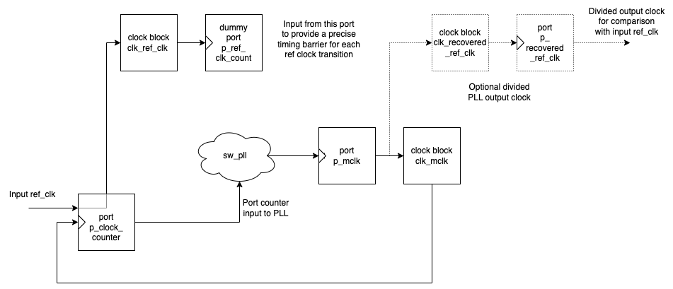
Use of Ports and Clock Blocks in the simple examples#
I²S slave example resource setup#
The I²S slave component already uses a clock block which captures the bit clock input. In addition to this, the PLL output is used to clock a dummy port’s counter which is used as the input to the PFD.
Since the precise sampling time of the PLL output clock count is variable due to instruction timing between the I²S LRCLK transition and the capture of the PLL output clock count in the I²S callback, an additional dummy port is used. This precisely synchronises the capture of the PLL output clock count relative to the BCLK transition and the relationship between these is used to reconstruct the absolute frequency difference with minimal input jitter.
fig_resources_i2s shows the resource arrangement of the I2S slave example.
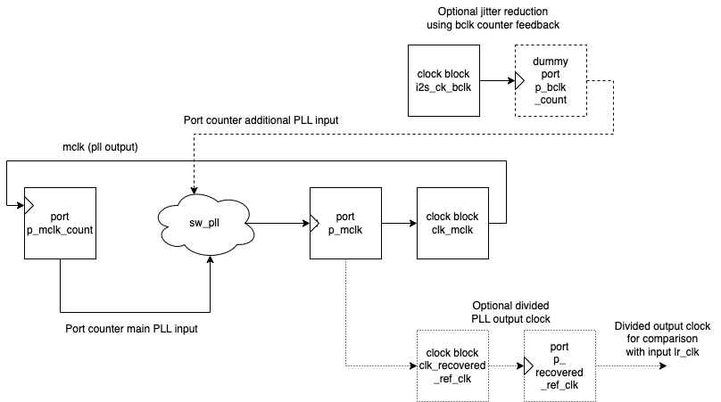
Use of Ports and Clock Blocks in the I²S slave example#
Software PLL API#
The Application Programmer Interface (API) for the Software PLL is shown below. It is split into items specific to LUT and SDM DCOs .
In addition to the standard API which takes a clock counting input (implements the PFD), for applications where the PLL is to be controlled using an alternatively derived error input, a low-level API is also provided. This low-level API allows the Software PLL to track an arbitrary clock source which is calculated by other means such as timing of received packets over a communications interface.
LUT Based PLL API#
The LUT based API are functions designed to be called from an audio loop. Typically the functions can take up to 210 instruction cycles when control occurs and just a few 10s of cycles when control does not occur. If run at a rate of 48 kHz then it will consume approximately 1 MIPS on average.
Warning
doxygengroup: Cannot find group “sw_pll_lut” in doxygen xml output for project “sln_voice” from directory: /build/doc/_build/_doxygen/sln_voice/xml
SDM Based PLL API#
All SDM API items are function calls. The SDM API requires a dedicated logical core to perform the SDM calculation and periodic register write and it is expected that the user provide the fork (par) and call to the SDM.
A typical design idiom is to have the task running in a loop with a timing barrier (either 1 us or 2 us depending on profile used) and a non-blocking channel poll which allows new DCO control values to be received as needed at the control loop rate. The SDM calculation and register write takes 45 instruction cycles and so with the overheads of the timing barrier and the non-blocking channel receive poll, a minimum 60 MHz logical core should be set aside for the SDM task running at 1 us period. This can be approximately halved it running at 2 us SDM period.
The control part of the SDM SW PLL takes 75 instruction cycles when active and a few 10 s of cycles when inactive so you will need to budget around 1 MIPS for this when being called at 48 kHz with a control rate of one in every 512 cycles.
An example of how to implement the threading, timing barrier and non-blocking channel poll can be found in examples/simple_sdm/simple_sw_pll_sdm.c. A thread diagram of how this can look is shown below.
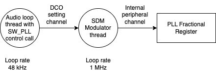
Example Thread Diagram of SDM SW PLL#
Warning
doxygengroup: Cannot find group “sw_pll_sdm” in doxygen xml output for project “sln_voice” from directory: /build/doc/_build/_doxygen/sln_voice/xml
Common API#
Warning
doxygengroup: Cannot find group “sw_pll_common” in doxygen xml output for project “sln_voice” from directory: /build/doc/_build/_doxygen/sln_voice/xml
Building and running the examples#
This section assumes you have downloaded and installed the XMOS XTC tools (see README for required version). Installation instructions can be found here.
Particular attention should be paid to the section Installation of required third-party tools.
The application examples uses the xcommon-cmake build system as bundled with the XTC tools.
To build the applications, from an XTC command prompt run the following commands in the lib_sw_pll/examples directory:
cmake -B build -G "Unix Makefiles"
xmake -C build
To run the firmware, first connect LRCLK and BCLK (connects the test clock output to the PLL reference input) and run one of the following commands. app_simple_lut or app_simple_sdm runs on the XK-EVK-XU316 board, app_i2s_slave_lut requires the XK-VOICE-SQ66 board:
xrun --xscope app_simple_lut/bin/app_simple_lut.xe
xrun --xscope app_simple_sdm/bin/app_simple_sdm.xe
xrun --xscope app_i2s_slave_lut/bin/app_i2s_slave_lut.xe
For app_simple_lut.xe and app_simple_sdm.xe, to see the PLL lock, put a oscilloscope probe on either LRCLK/BCLK (reference input) and another on PORT_I2S_DAC_DATA to see the recovered clock which has been hardware divided back down to the same rate as the input reference clock.
For i2s_slave_lut.xe you will need to connect a 48 kHz I²S master to the LRCLK, BCLK pins. You may then observe the I²S input data being looped back to the output and the MCLK being generated. A divided version of MCLK is output on PORT_I2S_DATA2 which allows direct comparison of the input reference (LRCLK) with the recovered clock at the same, and locked, frequency.