Device Pinout#
Pin Configuration#
The pinout of the XVF3800, including all optional interfaces, is shown in the figure below. Some of the pin descriptions indicate how these pins are allocated on the XMOS XK-VOICE-SQ66 development kit development kit (DVK), but they can be re-configured in the firmware for other uses.
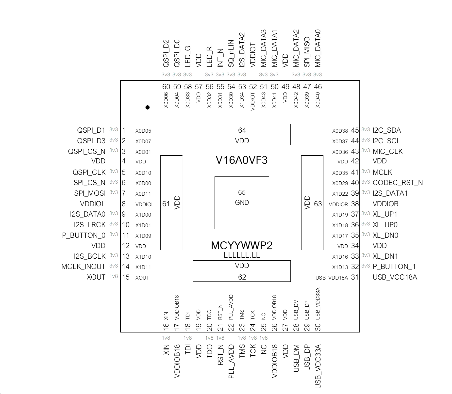
VDDIOT, VDDIOL and VDDIOR must be connected a 3V3 supply. VDDIO18 must be connected to a 1V8 supply, and all VDD pins must be connected to a 0V9 supply. All package paddles (pins 61 through 65) must be connected. It is advised to place a via under each paddle to connect it directly to a PCB supply plane.
Signal Description#
The table below lists the functions of all the pins above in the order they appear around the package.
Pin# |
Pin name |
Signal name |
Description |
Comments |
Dir (I/O) |
Power rail |
|---|---|---|---|---|---|---|
1 |
X0D05 |
QSPI_D1 |
QSPI Data Line 1 and boot selection. |
If pin is tied high via a 4.7k ohm resistor on startup the device will start in SPI slave boot mode. If the pin is left floating or connected to a quad SPI D1 pin on a memory device the device will start in QSPI master mode and attempt to boot from QSPI flash memory. |
I / O |
IOL |
2 |
X0D07 |
QSPI_D3 |
QSPI Data Line 3 |
I / O |
IOL |
|
3 |
X0D01 |
QSPI_CS_N |
QSPI Boot Flash - Chip Select |
Pull high externally to the device using a 4.7k ohm resistor |
O |
IOL |
5 |
X0D10 |
QSPI_CLK |
QSPI Clock |
O |
IOL |
|
6 |
X0D00 |
SPI_CS_N |
Slave SPI boot / Peripheral SPI Master Chip Select |
Pull high externally to the device using a 4.7k ohm resistor |
I |
IOL |
7 |
X0D11 |
SPI_MOSI |
SPI Master Out Slave In |
I |
IOL |
|
8 |
VDDIOL |
VDDIOL |
I/O Power Supply (3V3) |
All VDD pins must be connected. |
PWR |
|
9 |
X1D00 |
I2S_DATA0 |
I2S Data |
Reference input in INT-Device configuration / Output in USB and INT-Host configurations |
I / O |
IOL |
10 |
X1D01 |
I2S_LRCK |
I2S Left/Right clock |
48 kHz or 16 kHz clock derived as I2S_BLCK/64. |
O (master) / I (slave) |
IOL |
11 |
X1D09 |
P_BUTTON_0 |
Button input 0 |
Active low with 10k pullup on DVK |
I |
IOL |
13 |
X1D10 |
I2S_BCLK |
I2S bit synchronisation clock |
Configurable for 16 kHz (1.024 MHz) and 48 kHz (3.072 MHz) sample rates |
O (master) / I (slave) |
IOL |
14 |
X1D11 |
MCLK_INOUT |
Master audio clock |
An output copy of the internally generated MCLK. Must be connected to Pin 41. On ‘extmclk’ INT-Device configurations, an input pin accepting an external MCLK. |
I / O |
IOL |
15 |
XOUT |
XOUT |
Crystal oscillator output |
Note that this pin should be left floating when using the CMOS clock input |
O |
IOB |
16 |
XIN |
XIN |
Crystal oscillator input |
Alternatively this can be used as a clock input |
I |
IOB |
17 |
VDDIOB18 |
VDDIOB18 |
I/O Power Supply (1v8) |
1V8 supply must be connected. |
PWR |
|
18 |
TDI |
TDI |
JTAG test data input |
This pin has a weak internal pull-up. See note on debug headers. |
I |
IOB |
20 |
TDO |
TDO |
JTAG test data output |
O |
IOB |
|
21 |
RST_N |
RST_N |
Device reset |
Active low. This pin has a Schmitt trigger input and an internal weak pull up |
I |
IOB |
22 |
PLL_AVDD |
PLL_AVDD |
Analogue power supply for core and application PLL. |
Use a filtered version of the core supply as per the XU316-1024-QF60B datasheet. |
PWR |
|
23 |
TMS |
TMS |
JTAG test mode select |
This pin has a weak internal pull-up. See note on debug headers. |
I |
IOB |
24 |
TCK |
TCK |
JTAG test clock input |
This pin has a Schmitt trigger input and an internal weak pull-down. See note on debug headers. |
I |
IOB |
25 |
NC |
NC |
No Connection |
Not connected. This pin MUST NOT be connected to any net |
NA |
IOB |
26 |
VDDIOB18 |
VDDIOB18 |
I/O Power Supply (1v8) |
1V8 supply must be connected. |
PWR |
|
28 |
USB_DM |
USB_DM |
USB D- line |
May be left floating if USB is not required |
I / O |
|
29 |
USB_DP |
USB_DP |
USB D+ line |
May be left floating if USB is not required |
I / O |
|
30 |
USB_VDD33A |
USB_VCC33A |
3.3V power for the USB transceiver. |
May be left floating if USB is not required |
PWR |
|
31 |
USB_VDD18A |
USB_VCC18A |
1.8V power for the USB transceiver. |
May be left floating if USB is not required |
PWR |
|
32 |
X1D13 |
P_BUTTON_1 |
Button input 1 |
Active low with 10k pullup on DVK |
I |
IOR |
33 |
X1D16 |
XL_DN1 |
XLINK |
The 4 XL_DNx signals form a single 2-wire xlink connection for advanced debug only |
I |
IOR |
35 |
X1D17 |
XL_DN0 |
XLINK |
Debug port |
I |
IOR |
36 |
X1D18 |
XL_UP0 |
XLINK |
Debug port |
O |
IOR |
37 |
X1D19 |
XL_UP1 |
XLINK |
Debug port |
O |
IOR |
38 |
VDDIOR |
VDDIOR |
I/O Power Supply (3V3) |
All VDD pins must be connected. |
PWR |
|
39 |
X1D22 |
I2S_DATA1 |
I2S Data |
Audio data out to host processor in INT-Device config. Optional reference input in INT-Host config |
I / O |
IOR |
40 |
X0D29 |
CODEC _RST_N |
GPO for driving reset of conected DAC or digital amplifier |
O |
IOR |
|
41 |
X0D35 |
MCLK |
Master audio clock input used for generating PDM MIC clock |
Audio clock input to tile 0. Connect to MCLK_INOUT (Pin 14) |
I |
IOR |
43 |
X0D36 |
MIC_CLK |
Microphone clock output |
3.072 MHz output to PDM microphones |
O |
IOR |
44 |
X0D37 |
I2C_SCL |
I2C serial clock |
I2C serial clock line for receiving control command from I2C host or controlling DAC (depending on config) |
I / O |
IOR |
45 |
X0D38 |
I2C_SDA |
I2C serial data |
I2C serial data line for receiving control command from I2C host or controlling DAC (depending on config) |
I / O |
IOR |
46 |
X0D40 |
MIC_DATA0 |
Microphone input 0 |
Single data rate |
I |
IOT |
47 |
X0D39 |
SPI_MISO |
SPI Master In Slave Out. |
Only used when XVF3800 is a SPI controlled device. Not used by SPI slave boot. |
O |
IOT |
48 |
X0D42 |
MIC_DATA2 |
Microphone input 2 |
Single data rate |
I |
IOT |
50 |
X0D41 |
MIC_DATA1 |
Microphone input 1 |
Single data rate |
I |
IOT |
51 |
X0D43 |
MIC_DATA3 |
Microphone input 3 |
Single data rate |
I |
IOT |
52 |
VDDIOT |
VDDIOT |
I/O Power Supply (3V3) |
All VDD pins must be connected. |
PWR |
|
53 |
X1D34 |
I2S_DATA2 |
I2S Data |
Optional third I2S data line for forwarding processed far-end in INT-Device config. Connected to aux input of DAC on DVK to allow SW configurability. May be used as a GPIO when not assigned to I2S |
O |
IOT |
54 |
X0D30 |
SQ_nLIN |
GPO for selecting topology mode of mics on DVK |
O |
IOT |
|
55 |
X0D31 |
INT_N |
GPO for signalling an interrupt to the host |
O |
IOT |
|
56 |
X0D32 |
LED_R |
Red element of tri-colour LED on DVK |
O |
IOT |
|
58 |
X0D33 |
LED_G |
Green element of tri-colour LED on DVK |
O |
IOT |
|
59 |
X0D04 |
QSPI_D0 |
QSPI Boot Flash / QSPI Data Line 0 |
I / O |
IOL |
|
60 |
X0D06 |
QSPI_D2 |
QSPI Data Line 2 |
I / O |
IOL |
|
65 |
GND |
GND |
Ground |
All package paddles must be connected. It is advised that vias be placed under paddles to connect directly to PCB supply planes |
GND |
|
61, 62, 63, 64 |
VDD |
VDD |
Core power supply (0v9) |
All package paddles must be connected. It is advised that vias be placed under paddles to connect directly to PCB supply planes |
PWR |
|
4, 12, 19, 27, 34, 42, 49, 57 |
VDD |
VDD |
Core power supply (0v9) |
All VDD pins must be connected. |
PWR |
Note
All VDD pins must be connected, excluding the USB_VDD supplies which can be left floating if USB is not required.
VDDIOT, VDDIOL and VDDIOR must be connected to a 3V3 supply.
VDDIO18 must be connected to a 1V8 supply.
All package paddles must be connected. It is advised to place a via under each paddle to connect directly to a PCB supply plane.
The function of some pins change depending on the firmware configuration loaded during boot.