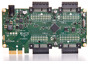
L16 sliceKIT core board
The L16 core board board contains the xCORE device plus support circuitry.
A single XS1-L16-128-QF124 device has all of its GPIO connected to the slots.
Multiple core boards
Additional sliceKIT core boards can be connected to the Chain slot on the first board via the Square Slot on the second board, to add extra processing capability and I/O through extra sliceCARDs. The first board is termed the Master and the remaining boards are Slaves. When there is only one board, it is the Master.
Setup
For debugging, an xSYS adaptor board is connected to the Chain connector of the Master board to allow connection of an xTAG-2 which provides a debug link from a USB host.
The core board is powered by a 12V external power supply.
Power supply
Power input to the sliceKIT core board is via a standard barrel jack connector. A standard 12V external power supply should be used to power the board. Each core board requires its own 12V supply. This input supply is used to generate the main 5V board supply via a DC-DC converter.
The 5V board supply is then fed to all the slot connectors as well as powering the core board itself. 3V3 and 1V0 supplies are be generated by DC-DC converters from the 5V main supply.
The supplies are sequenced to ensure the power up sequence is 5V then 3V3 then 1V0. When the 1V0 supply is good, the system is released from reset.
The core board provides 3V3 and 5V at 0.25A each for a total of approximately 2W per slice.
Debug
Debug of the system is via the xSYS adapter board connected to the Chain connector.
The JTAG signals are connected as shown below.
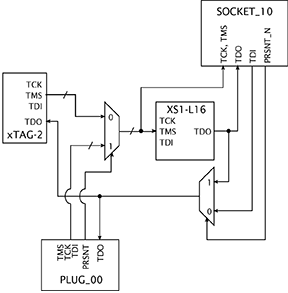
Presence detect signals are present on both the Chain connector and Square slot connectors to allow detection of a connected board and subsequent automatic switching of the JTAG chain. In a system of multiple core boards, the Master is the source of the JTAG chain so the system can only be debugged from the master. Other boards will see no devices in the JTAG chain.
The use of xSCOPE is covered in the xCONNECT Links section. The xSCOPE xCONNECT Link can be either enabled or disabled via a switch on the xSYS adapter board.
XS1-L16 boot
Master core boards boot from SPI flash, while slave core boards boot from xCONNECT link XLB from the next connected core board.
To allow re-use of the SPI boot pins (ports 1A, 1B, 1C, 1D) as signal I/O pins for the Star slot, a latched bus switch is used which connects the xCORE SPI pins to either the SPI Flash or to the sliceCARD slots. The switch is controlled by X0D42 and X0D43 (P8D6 and P8D7 on Tile 0 - on the Triangle slot). Once the device has booted, X0D43 is used to enable or disable the SPI interface, X0D42 should then transition from low to high to latch the selection. The SPI selection state is maintained until the system is reset.
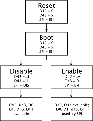
Once this sequence is completed and the selection has been latched, X0D42 and X0D43 return to performing their normal functions in the Triangle slot.
If the SPI is not disabled, then SliceCARDs in the Star slot may not function as expected. If there is no sliceCARD in the Star slot, then it does not matter whether the SPI has been disabled or not. Therefore, applications which require runtime access to the SPI flash should either leave the Star slot unpopulated or check to ensure that the sliceCARD which is in the slot will be unaffected by the operation of the flash device.
The xTAG-2 system can use the boot mode select signal to force all devices in the chain (master and slave core boards) to boot from JTAG (don’t boot) for debug purposes.
If not in this mode, the devices will boot from SPI or xCONNECT Link as appropriate.
xCONNECT Links
The Chain connector contains two 5-bit xCONNECT Links, XLA and XLB, which can be used to chain sliceKIT core boards together. The links from Tile 0 are connected to the Chain connector and the Star slot. The links from Tile 1 are connected to the Square slot.
The only complication in this system is use of the xSCOPE 2-bit xCONNECT Link. This link overlaps a 4 bit port on the Star slot connector so it is not possible to use this for user I/O at the same time as xSCOPE.
To work around this, a switch is present on the xSYS adapter board to either enable or disable the xSCOPE xCONNECT Link. When disabled, these pins are disconnected from the Chain connector and are free for use on the Star slot. When enabled they will work as an xCONNECT Link and hence appear on the relevant pins of the Star slot.
It is recommended that if a sliceCARD is used in the Star Slot the XSCOPE switch is off on the xSYS adaptor card to ensure correct operation of the sliceCARD in the Star slot.
Reset
The whole system is held in reset until all power supplies are stable, and reset is connected to all Slice Cards so any circuitry on them can be reset. Reset also indicates to the sliceCARDs that their power input is stable. The reset from the xTAG-2 resets the whole system, if required for debugging.
Clocking
The system clock has two sources: an on-board 25MHz oscillator or the CLK signal from the Chain connector. The system clock source is selected automatically according to the presence of signals on the Chain connector.
This means the system clock from a Master core board is fed automatically to all of the slave core boards so the whole system will operate synchronously.
The system clock is also fed to each of the sliceCARD slots.
Testpoints
Each xCORE I/O signal is also available on a 0.1” header, next to the slot that it is connected to. These connections can be used to connect an oscilloscope or logic analyser, or for interconnection of signals for advanced development work.
The signals are identified on the silkscreen layer of the sliceKIT core board; the table below lists their relationship to the internal ports.
L16 Pin |
Slot |
PCIE |
Function |
||||
|---|---|---|---|---|---|---|---|
X0D0 |
TRIANGLE |
B2 |
P1A0 |
||||
X0D1 |
STAR |
A8 |
P1B0 |
||||
CHAIN |
B10 |
||||||
X0D2 |
STAR |
B6 |
P4A0 |
P8A0 |
P16A0 |
P32A20 |
|
CHAIN |
A7 |
||||||
X0D3 |
STAR |
B7 |
P4A1 |
P8A1 |
P16A1 |
P32A21 |
|
CHAIN |
A6 |
||||||
X0D4 |
STAR |
B9 |
P4B0 |
P8A2 |
P16A2 |
P32A22 |
|
CHAIN |
A11 |
||||||
X0D5 |
STAR |
B11 |
P4B1 |
P8A3 |
P16A3 |
P32A23 |
|
CHAIN |
A9 |
||||||
X0D6 |
STAR |
A9 |
P4B2 |
P8A4 |
P16A4 |
P32A24 |
|
CHAIN |
B11 |
||||||
X0D7 |
STAR |
A11 |
P4B3 |
P8A5 |
P16A5 |
P32A25 |
|
CHAIN |
B9 |
||||||
X0D8 |
STAR |
A6 |
P4A2 |
P8A6 |
P16A6 |
P32A26 |
|
CHAIN |
B7 |
||||||
X0D9 |
STAR |
A7 |
P4A3 |
P8A7 |
P16A7 |
P32A27 |
|
CHAIN |
B6 |
||||||
X0D10 |
STAR |
B10 |
P1C0 |
||||
CHAIN |
A8 |
||||||
X0D11 |
TRIANGLE |
B4 |
P1D0 |
||||
X0D12 |
TRIANGLE |
A3 |
P1E0 |
||||
X0D13 |
STAR |
A15 |
P1F0 |
||||
CHAIN |
B15 |
||||||
X0D14 |
STAR |
B12 |
P4C0 |
P8B0 |
P16A8 |
P32A28 |
|
CHAIN |
A13 |
||||||
X0D15 |
STAR |
B13 |
P4C1 |
P8B1 |
P16A9 |
P32A29 |
|
CHAIN |
A12 |
||||||
X0D16 |
STAR |
B17 |
P4D0 |
P8B2 |
P16A10 |
||
CHAIN |
A18 |
||||||
X0D17 |
STAR |
B18 |
P4D1 |
P8B3 |
P16A11 |
||
CHAIN |
A17 |
||||||
X0D18 |
STAR |
A17 |
P4D2 |
P8B4 |
P16A12 |
||
CHAIN |
B18 |
||||||
X0D19 |
STAR |
A18 |
P4D3 |
P8B5 |
P16A13 |
||
CHAIN |
B17 |
||||||
X0D20 |
STAR |
A12 |
P4C2 |
P8B6 |
P16A14 |
P32A30 |
|
CHAIN |
B13 |
||||||
X0D21 |
STAR |
A13 |
P4C3 |
P8B7 |
P16A15 |
P32A31 |
|
CHAIN |
B12 |
||||||
X0D22 |
STAR |
B15 |
P1G0 |
||||
CHAIN |
A15 |
||||||
X0D23 |
TRIANGLE |
A4 |
P1H0 |
||||
X0D24 |
TRIANGLE |
B15 |
P1I0 |
||||
X0D25 |
TRIANGLE |
A8 |
P1J0 |
||||
X0D26 |
TRIANGLE |
B6 |
P4E0 |
P8C0 |
P16B0 |
||
X0D27 |
TRIANGLE |
B7 |
P4E1 |
P8C1 |
P16B1 |
||
X0D28 |
TRIANGLE |
B9 |
P4F0 |
P8C2 |
P16B2 |
||
X0D29 |
TRIANGLE |
B11 |
P4F1 |
P8C3 |
P16B3 |
||
X0D30 |
TRIANGLE |
A9 |
P4F2 |
P8C4 |
P16B4 |
||
X0D31 |
TRIANGLE |
A11 |
P4F3 |
P8C5 |
P16B5 |
||
X0D32 |
TRIANGLE |
A6 |
P4E2 |
P8C6 |
P16B6 |
||
X0D33 |
TRIANGLE |
A7 |
P4E3 |
P8C7 |
P16B7 |
||
X0D34 |
TRIANGLE |
B10 |
P1K0 |
||||
X0D35 |
TRIANGLE |
A15 |
P1L0 |
||||
X0D36 |
TRIANGLE |
B12 |
P1M0 |
P8D0 |
P16B8 |
||
X0D37 |
TRIANGLE |
B13 |
P1N0 |
P8D1 |
P16B9 |
||
X0D38 |
TRIANGLE |
B17 |
P1O0 |
P8D2 |
P16B10 |
||
X0D39 |
TRIANGLE |
B18 |
P1P0 |
P8D3 |
P16B11 |
||
X0D40 |
TRIANGLE |
A17 |
P8D4 |
P16B12 |
|||
X0D41 |
TRIANGLE |
A18 |
P8D5 |
P16B13 |
|||
X0D42 |
TRIANGLE |
A12 |
P8D6 |
P16B14 |
|||
X0D43 |
TRIANGLE |
A13 |
P8D7 |
P16B15 |
|||
X1D0 |
CIRCLE |
B2 |
P1A0 |
||||
X1D1 |
SQUARE |
A8 |
P1B0 |
||||
X1D2 |
SQUARE |
B6 |
P4A0 |
P8A0 |
P16A0 |
P32A20 |
|
X1D3 |
SQUARE |
B7 |
P4A1 |
P8A1 |
P16A1 |
P32A21 |
|
X1D4 |
SQUARE |
B9 |
P4B0 |
P8A2 |
P16A2 |
P32A22 |
|
X1D5 |
SQUARE |
B11 |
P4B1 |
P8A3 |
P16A3 |
P32A23 |
|
X1D6 |
SQUARE |
A9 |
P4B2 |
P8A4 |
P16A4 |
P32A24 |
|
X1D7 |
SQUARE |
A11 |
P4B3 |
P8A5 |
P16A5 |
P32A25 |
|
X1D8 |
SQUARE |
A6 |
P4A2 |
P8A6 |
P16A6 |
P32A26 |
|
X1D9 |
SQUARE |
A7 |
P4A3 |
P8A7 |
P16A7 |
P32A27 |
|
X1D10 |
SQUARE |
B10 |
P1C0 |
||||
X1D11 |
CIRCLE |
B4 |
P1D0 |
||||
X1D12 |
CIRCLE |
A3 |
P1E0 |
||||
X1D13 |
SQUARE |
A15 |
P1F0 |
||||
X1D14 |
SQUARE |
B12 |
P4C0 |
P8B0 |
P16A8 |
P32A28 |
|
X1D15 |
SQUARE |
B13 |
P4C1 |
P8B1 |
P16A9 |
P32A29 |
|
X1D16 |
SQUARE |
B17 |
P4D0 |
P8B2 |
P16A10 |
||
X1D17 |
SQUARE |
B18 |
P4D1 |
P8B3 |
P16A11 |
||
X1D18 |
SQUARE |
A17 |
P4D2 |
P8B4 |
P16A12 |
||
X1D19 |
SQUARE |
A18 |
P4D3 |
P8B5 |
P16A13 |
||
X1D20 |
SQUARE |
A12 |
P4C2 |
P8B6 |
P16A14 |
P32A30 |
|
X1D21 |
SQUARE |
A13 |
P4C3 |
P8B7 |
P16A15 |
P32A31 |
|
X1D22 |
SQUARE |
B15 |
P1G0 |
||||
X1D23 |
CIRCLE |
A4 |
P1H0 |
||||
X1D24 |
CIRCLE |
B15 |
P1I0 |
||||
X1D25 |
CIRCLE |
A8 |
P1J0 |
||||
X1D26 |
CIRCLE |
B6 |
P4E0 |
P8C0 |
P16B0 |
||
X1D27 |
CIRCLE |
B7 |
P4E1 |
P8C1 |
P16B1 |
||
X1D28 |
CIRCLE |
B9 |
P4F0 |
P8C2 |
P16B2 |
||
X1D29 |
CIRCLE |
B11 |
P4F1 |
P8C3 |
P16B3 |
||
X1D30 |
CIRCLE |
A9 |
P4F2 |
P8C4 |
P16B4 |
||
X1D31 |
CIRCLE |
A11 |
P4F3 |
P8C5 |
P16B5 |
||
X1D32 |
CIRCLE |
A6 |
P4E2 |
P8C6 |
P16B6 |
||
X1D33 |
CIRCLE |
A7 |
P4E3 |
P8C7 |
P16B7 |
||
X1D34 |
CIRCLE |
B10 |
P1K0 |
||||
X1D35 |
CIRCLE |
A15 |
P1L0 |
||||
X1D36 |
CIRCLE |
B12 |
P1M0 |
P8D0 |
P16B8 |
||
X1D37 |
CIRCLE |
B13 |
P1N0 |
P8D1 |
P16B9 |
||
X1D38 |
CIRCLE |
B17 |
P1O0 |
P8D2 |
P16B10 |
||
X1D39 |
CIRCLE |
B18 |
P1P0 |
P8D3 |
P16B11 |
||
Slot pinouts
The signal assignments for the connectors on the core board and sliceCARDs are shown in the table below.
STAR
PCIE B (TOP) |
SIGNAL |
FUNCTION |
||||
|---|---|---|---|---|---|---|
B1 |
NC |
NOT CONNECTED |
||||
B2 |
NC |
NOT CONNECTED |
||||
B3 |
GND |
POWER SUPPLY GROUND |
||||
B4 |
NC |
NOT CONNECTED |
||||
B5 |
3V3 |
POWER SUPPLY 3.3V |
||||
B6 |
X0D2 |
P4A0 |
P8A0 |
P16A0 |
P32A20 |
|
B7 |
X0D3 |
P4A1 |
P8A1 |
P16A1 |
P32A21 |
|
B8 |
GND |
POWER SUPPLY GROUND |
||||
B9 |
X0D4 |
P4B0 |
P8A2 |
P16A2 |
P32A22 |
|
B10 |
X0D10 |
P1C0 |
||||
B11 |
X0D3 |
P4B1 |
P8A3 |
P16A3 |
P32A23 |
|
KEY |
KEY |
MECHANICAL KEY |
||||
B12 |
X0D14 |
P4C0 |
P8B0 |
P16A8 |
P32A28 |
|
B13 |
X0D15 |
P4C1 |
P8B1 |
P16A9 |
P32A29 |
|
B14 |
CLK |
MAIN SYSTEM CLOCK |
||||
B15 |
X0D22 |
P1G0 |
||||
B16 |
GND |
POWER SUPPLY GROUND |
||||
B17 |
X0D16 |
P4D0 |
P8B2 |
P16A10 |
||
B18 |
X0D17 |
P4D1 |
P8B3 |
P16A11 |
||
PCIE A (BOT) |
SIGNAL |
FUNCTION |
||||
|---|---|---|---|---|---|---|
A1 |
NC |
NOT CONNECTED |
||||
A2 |
5V |
POWER SUPPLY 5V |
||||
A3 |
NC |
NOT CONNECTED |
||||
A4 |
NC |
NOT CONNECTED |
||||
A5 |
GND |
POWER SUPPLY GROUND |
||||
A6 |
X0D8 |
P4A2 |
P8A6 |
P16A6 |
P32A26 |
|
A7 |
X0D9 |
P4A3 |
P8A7 |
P16A7 |
P32A27 |
|
A8 |
X0D1 |
P1B0 |
||||
A9 |
X0D6 |
P4B2 |
P8A4 |
P16A4 |
P32A24 |
|
A10 |
GND |
POWER SUPPLY GROUND |
||||
A11 |
X0D7 |
P4B3 |
P8A5 |
P16A5 |
P32A25 |
|
KEY |
KEY |
MECHANICAL KEY |
||||
A12 |
X0D20 |
P4C2 |
P8B6 |
P16A14 |
P32A30 |
|
A13 |
X0D21 |
P4C3 |
P8B7 |
P16A15 |
P32A31 |
|
A14 |
GND |
POWER SUPPLY GROUND |
||||
A15 |
X0D13 |
P1F0 |
||||
A16 |
RST_N |
SYSTEM RESET (ACTIVE LOW) |
||||
A17 |
X0D18 |
P4D2 |
P8B4 |
P16A12 |
||
A18 |
X0D19 |
P4D3 |
P8B5 |
P16A13 |
||
SQUARE
PCIE B (TOP) |
SIGNAL |
FUNCTION |
||||
|---|---|---|---|---|---|---|
B1 |
DEBUG |
XSYS DEBUG SIGNAL |
||||
B2 |
TCK |
XSYS TCK SIGNAL |
||||
B3 |
GND |
POWER SUPPLY GROUND |
||||
B4 |
TDI |
XSYS TDI SIGNAL |
||||
B5 |
3V3 |
POWER SUPPLY 3.3V |
||||
B6 |
X1D2 |
P4A0 |
P8A0 |
P16A0 |
P32A20 |
|
B7 |
X1D3 |
P4A1 |
P8A1 |
P16A1 |
P32A21 |
|
B8 |
GND |
POWER SUPPLY GROUND |
||||
B9 |
X1D4 |
P4B0 |
P8A2 |
P16A2 |
P32A22 |
|
B10 |
X1D10 |
P1C0 |
||||
B11 |
X1D3 |
P4B1 |
P8A3 |
P16A3 |
P32A23 |
|
KEY |
KEY |
MECHANICAL KEY |
||||
B12 |
X1D14 |
P4C0 |
P8B0 |
P16A8 |
P32A28 |
|
B13 |
X1D15 |
P4C1 |
P8B1 |
P16A9 |
P32A29 |
|
B14 |
CLK |
MAIN SYSTEM CLOCK |
||||
B15 |
X1D22 |
P1G0 |
||||
B16 |
GND |
POWER SUPPLY GROUND |
||||
B17 |
X1D16 |
P4D0 |
P8B2 |
P16A10 |
||
B18 |
X1D17 |
P4D1 |
P8B3 |
P16A11 |
||
PCIE A (BOT) |
SIGNAL |
FUNCTION |
||||
|---|---|---|---|---|---|---|
A1 |
MSEL |
XYSY MSEL SIGNAL |
||||
A2 |
5V |
POWER SUPPLY 5V |
||||
A3 |
TMS |
XSYS TMS SIGNAL |
||||
A4 |
TDO |
XSYS TDO SIGNAL |
||||
A5 |
PRSNT |
SYSTEM PRESENT SIGNAL (ACTIVE LOW) |
||||
A6 |
X1D8 |
P4A2 |
P8A6 |
P16A6 |
P32A26 |
|
A7 |
X1D9 |
P4A3 |
P8A7 |
P16A7 |
P32A27 |
|
A8 |
X1D1 |
P1B0 |
||||
A9 |
X1D6 |
P4B2 |
P8A4 |
P16A4 |
P32A24 |
|
A10 |
GND |
POWER SUPPLY GROUND |
||||
A11 |
X1D7 |
P4B3 |
P8A5 |
P16A5 |
P32A25 |
|
KEY |
KEY |
MECHANICAL KEY |
||||
A12 |
X1D20 |
P4C2 |
P8B6 |
P16A14 |
P32A30 |
|
A13 |
X1D21 |
P4C3 |
P8B7 |
P16A15 |
P32A31 |
|
A14 |
GND |
POWER SUPPLY GROUND |
||||
A15 |
X1D13 |
P1F0 |
||||
A16 |
RST_N |
SYSTEM RESET (ACTIVE LOW) |
||||
A17 |
X1D18 |
P4D2 |
P8B4 |
P16A12 |
||
A18 |
X1D19 |
P4D3 |
P8B5 |
P16A13 |
||
TRIANGLE
PCIE B (TOP) |
SIGNAL |
FUNCTION |
||||
|---|---|---|---|---|---|---|
B1 |
NC |
NOT CONNECTED |
||||
B2 |
X0D0 |
P1A0 |
||||
B3 |
GND |
POWER SUPPLY GROUND |
||||
B4 |
X0D11 |
P1D0 |
||||
B5 |
3V3 |
POWER SUPPLY 3.3V |
||||
B6 |
X0D26 |
P4E0 |
P8C0 |
P16B0 |
||
B7 |
X0D27 |
P4E1 |
P8C1 |
P16B1 |
||
B8 |
GND |
POWER SUPPLY GROUND |
||||
B9 |
X0D28 |
P4F0 |
P8C2 |
P16B2 |
||
B10 |
X0D34 |
P1K0 |
||||
B11 |
X0D29 |
P4F1 |
P8C3 |
P16B3 |
||
KEY |
KEY |
MECHANICAL KEY |
||||
B12 |
X0D36 |
P1M0 |
P8D0 |
P16B8 |
||
B13 |
X0D37 |
P1N0 |
P8D1 |
P16B9 |
||
B14 |
CLK |
MAIN SYSTEM CLOCK |
||||
B15 |
X0D24 |
P1I0 |
||||
B16 |
GND |
POWER SUPPLY GROUND |
||||
B17 |
X0D38 |
P1O0 |
P8D2 |
P16B10 |
||
B18 |
X0D39 |
P1P0 |
P8D3 |
P16B11 |
||
PCIE A (BOT) |
SIGNAL |
FUNCTION |
||||
|---|---|---|---|---|---|---|
A1 |
NC |
NOT CONNECTED |
||||
A2 |
5V |
POWER SUPPLY 5V |
||||
A3 |
X0D12 |
P1E0 |
||||
A4 |
X0D23 |
P1H0 |
||||
A5 |
GND |
POWER SUPPLY GROUND |
||||
A6 |
X0D32 |
P4E2 |
P8C6 |
P16B6 |
||
A7 |
X0D33 |
P4E3 |
P8C7 |
P16B7 |
||
A8 |
X0D25 |
P1J0 |
||||
A9 |
X0D30 |
P4F2 |
P8C4 |
P16B4 |
||
A10 |
GND |
POWER SUPPLY GROUND |
||||
A11 |
X0D31 |
P4F3 |
P8C5 |
P16B5 |
||
KEY |
KEY |
MECHANICAL KEY |
||||
A12 |
X0D42 |
P8D6 |
P16B14 |
|||
A13 |
X0D43 |
P8D7 |
P16B15 |
|||
A14 |
GND |
POWER SUPPLY GROUND |
||||
A15 |
X0D35 |
P1L0 |
||||
A16 |
RST_N |
SYSTEM RESET (ACTIVE LOW) |
||||
A17 |
X0D40 |
P8D4 |
P16B12 |
|||
A18 |
X0D41 |
P8D5 |
P16B13 |
|||
CIRCLE
PCIE B (TOP) |
SIGNAL |
FUNCTION |
||||
|---|---|---|---|---|---|---|
B1 |
NC |
NOT CONNECTED |
||||
B2 |
X1D0 |
P1A0 |
||||
B3 |
GND |
POWER SUPPLY GROUND |
||||
B4 |
X1D11 |
P1D0 |
||||
B5 |
3V3 |
POWER SUPPLY 3.3V |
||||
B6 |
X1D26 |
P4E0 |
P8C0 |
P16B0 |
||
B7 |
X1D27 |
P4E1 |
P8C1 |
P16B1 |
||
B8 |
GND |
POWER SUPPLY GROUND |
||||
B9 |
X1D28 |
P4F0 |
P8C2 |
P16B2 |
||
B10 |
X1D34 |
P1K0 |
||||
B11 |
X1D29 |
P4F1 |
P8C3 |
P16B3 |
||
KEY |
KEY |
MECHANICAL KEY |
||||
B12 |
X1D36 |
P1M0 |
P8D0 |
P16B8 |
||
B13 |
X1D37 |
P1N0 |
P8D1 |
P16B9 |
||
B14 |
CLK |
MAIN SYSTEM CLOCK |
||||
B15 |
X1D24 |
P1I0 |
||||
B16 |
GND |
POWER SUPPLY GROUND |
||||
B17 |
X1D38 |
P1O0 |
P8D2 |
P16B10 |
||
B18 |
X1D39 |
P1P0 |
P8D3 |
P16B11 |
||
PCIE A (BOT) |
SIGNAL |
FUNCTION |
||||
|---|---|---|---|---|---|---|
A1 |
NC |
NOT CONNECTED |
||||
A2 |
5V |
POWER SUPPLY 5V |
||||
A3 |
X1D12 |
P1E0 |
||||
A4 |
X1D23 |
P1H0 |
||||
A5 |
GND |
POWER SUPPLY GROUND |
||||
A6 |
X1D32 |
P4E2 |
P8C6 |
P16B6 |
||
A7 |
X1D33 |
P4E3 |
P8C7 |
P16B7 |
||
A8 |
X1D25 |
P1J0 |
||||
A9 |
X1D30 |
P4F2 |
P8C4 |
P16B4 |
||
A10 |
GND |
POWER SUPPLY GROUND |
||||
A11 |
X1D31 |
P4F3 |
P8C5 |
P16B5 |
||
KEY |
KEY |
MECHANICAL KEY |
||||
A12 |
NC |
NOT CONNECTED |
||||
A13 |
NC |
NOT CONNECTED |
||||
A14 |
GND |
POWER SUPPLY GROUND |
||||
A15 |
X1D35 |
P1L0 |
||||
A16 |
RST_N |
SYSTEM RESET (ACTIVE LOW) |
||||
A17 |
NC |
NOT CONNECTED |
||||
A18 |
NC |
NOT CONNECTED |
||||
CHAIN
PCIE B (TOP) |
SIGNAL |
FUNCTION |
||||
|---|---|---|---|---|---|---|
B1 |
DEBUG |
XSYS DEBUG SINGAL |
||||
B2 |
TCK |
XSYS TCK SIGNAL |
||||
B3 |
GND |
POWER SUPPLY GROUND |
||||
B4 |
TDO |
XSYS TDO SIGNAL |
||||
B5 |
PRSNT |
CHAIN PRESENT SIGNAL |
||||
B6 |
X0D9 |
XLA4o |
XLA5b |
|||
B7 |
X0D8 |
XLA2i |
XLA5b |
|||
B8 |
GND |
POWER SUPPLY GROUND |
||||
B9 |
X0D7 |
XLA1i |
XLA2b |
XLA5b |
||
B10 |
X0D1 |
XLA4o |
XLA5b |
|||
B11 |
X0D6 |
XLA0i |
XLA2b |
XLA5b |
||
KEY |
KEY |
MECHANICAL KEY |
||||
B12 |
X0D21 |
XLB0i |
XLB2b |
XLB5b |
||
B13 |
X0D20 |
XLB2i |
XLB5b |
|||
B14 |
CLK |
MAIN SYSTEM CLOCK |
||||
B15 |
X0D13 |
XLB4o |
XLB5b |
|||
B16 |
GND |
POWER SUPPLY GROUND |
||||
B17 |
X0D19 |
XLB1i |
XLB2b |
XLB5b |
||
B18 |
X0D18 |
XLB0i |
XLB2b |
XLB5b |
||
PCIE A (BOT) |
SIGNAL |
FUNCTION |
||||
|---|---|---|---|---|---|---|
A1 |
MSEL |
XSYS MSEL SIGNAL |
||||
A2 |
NC |
NOT CONNECTED |
||||
A3 |
TMS |
XSYS TMS SIGNAL |
||||
A4 |
TDI |
XSYS TDI SIGNAL |
||||
A5 |
GND |
POWER SUPPLY GROUND |
||||
A6 |
X0D3 |
XLA2o |
XLA5b |
|||
A7 |
X0D2 |
XLA3o |
XLA5b |
|||
A8 |
X0D10 |
XLA4i |
XLA5b |
|||
A9 |
X0D5 |
XLA0o |
XLA2b |
XLA5b |
||
A10 |
GND |
POWER SUPPLY GROUND |
||||
A11 |
X0D4 |
XLA1o |
XLA2b |
XLA5b |
||
KEY |
KEY |
MECHANICAL KEY |
||||
A12 |
X0D15 |
XLB2o |
XLB5b |
|||
A13 |
X0D14 |
XLB3o |
XLB5b |
|||
A14 |
GND |
POWER SUPPLY GROUND |
||||
A15 |
X0D22 |
XLB4i |
XLB5b |
|||
A16 |
RST_N |
SYSTEM RESET (ACTIVE LOW) |
||||
A17 |
X0D17 |
XLB0o |
XLB2b |
XLB5b |
||
A18 |
X0D16 |
XLB1o |
XLB2b |
XLB5b |
||
System services slot signals
On all slots, TDO is always out of the sliceKIT core board, TDI is always in to the core board.
MSEL, TCK, TMS, RST_N are all inputs to the core board from the Chain connector and outputs from the core board on the Square slot.
DEBUG is bidirectional.
PRSNT is used on the Chain connector to detect it is plugged into the Square slot of another core board. This signal is used to switch JTAG and CLK sources. Similarly, PRSNT_N is used on the Star slot to detect another core board is connected. This signal is used to switch the JTAG chain signals.
CLK and RST_N are inputs to the core board from the Chain connector and output from all slots.