Switching characteristics
For clock, reset and JTAG timing refer to the XU316-1024-QF60(A/B) datasheet. XVF3610 specific interface timings are detailed below.
QSPI Master (External flash for boot image storage)
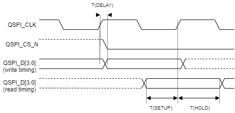
Fig. 16 QSPI Timing
Parameter |
Symbol |
Min |
Typical |
Max |
Units |
|---|---|---|---|---|---|
QSPI Clock frequency |
f(QSPI_CLK) |
TBC |
50 |
MHz |
|
QSPI_CLK to QSPI Data output delay |
T(DELAY) |
-2.7 |
2.7 |
ns |
|
QSPI Data input to QSPI_CLK Setup time |
T(SETUP) |
22 |
ns |
||
QSPI Data input to QSPI_CLK hold time |
T(HOLD) |
-11 |
ns |
I2S Slave
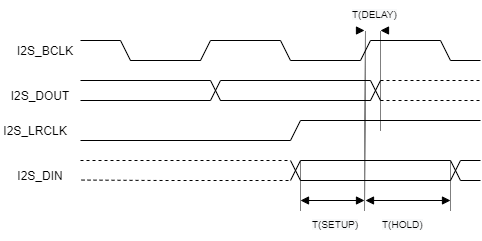
Fig. 17 I2S Slave timing
A: Configurable input multiplier used to generate appropriate audio sample rates (16kHz / 48kHz)
B: Timing also applies to I2S Sample Clock (I2S_LRCLK)
SPI Slave (External processor boot)
Parameter |
Symbol |
Min |
Typical |
Max |
Units |
Notes |
|---|---|---|---|---|---|---|
SPI Clock frequency |
f(SPI_CLK) |
TBC |
TBC |
MHz |
||
SPI_CLK to MISO output delay |
T(DELAY) |
11 |
21.3 |
ns |
||
SPI Master Output Slave Input (MOSI) to SPI_CLK Setup time |
T(SETUP) |
0 |
ns |
|||
SPI Master Output Slave Input to (MOSI) SPI_CLK hold time |
T(HOLD) |
6 |
ns |
A: Timing also applies to SPI Chip Select input (SPI_CS_N)
SPI Master (Peripheral control)
Parameter |
Symbol |
Min |
Typical |
Max |
Units |
Notes |
|---|---|---|---|---|---|---|
SPI Clock frequency |
f(SPI_CLK) |
TBC |
TBC |
MHz |
||
SPI_CLK to MISO output delay |
T(DELAY) |
11 |
21.3 |
ns |
||
SPI Master Output Slave Input (MOSI) to SPI_CLK Setup time |
T(SETUP) |
0 |
ns |
|||
SPI Master Output Slave Input to (MOSI) SPI_CLK hold time |
T(HOLD) |
6 |
ns |