Following our poster presentation on xcore.ai – our new crossover processor for the AIoT – at the 2020 tinyML summit, we were delighted to be invited back for a tinyML Talks webcast to demonstrate our software tools and share our vision of the future for hardware for edge AI devices. The ever-growing community of edge AI enthusiasts have been working hard to develop software and hardware that delivers high performance within the tight power budgets typically associated with battery operated devices. Consideration of computational throughput and energy efficiency is at the center of design efforts, but we want to emphasize an equally important, but often overlooked factor: cost.
Estimating the cost of any product featuring edge AI is a complicated task. Tradeoffs between software and hardware complexity, device size, eBOM, time to market and other technical and commercial parameters must be carefully balanced. Merely defining comparative cost metrics is difficult for the same reasons power benchmarks of edge AI devices are hard to interpret; the target domains of different devices are diverse (power ranging from nW to 100mw) with different levels of hardware and software integration requirements (from wake word detection ASICs, through neural accelerator IP for SOCs).
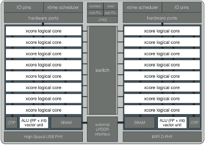
Our new chip aims to lower the total system cost and power requirements for consumer electronics devices by taking advantage of the flexibility and scalability of XMOS’ proprietary multicore instruction set, and a novel vector unit for edge inference tasks. Our platform allows for:
- Reducing eBOM and system complexity by replacing the application processor and IO processor with a single chip
- Implementing hardware interfaces through software, and only as needed (this is what xcore® processors have been designed for originally)
- Reducing silicon IP costs by in-house hardware design
- Keeping the die area small and manufacturing process inexpensive but performant
- Making neural network model deployment easy and computationally efficient across a wide variety of tasks (from tiny wake word models to face verifications systems with millions of parameters)

At the heart of the ML inference capabilities offered by xcore.ai lies the vector processing unit (VPU). To keep the system simple and the die area small, while retaining the hard-real-time guarantees of xcore processors, we decided to integrate the VPU closely with the rest of the ALU. This allows for reduced latency and increased throughput since there is no need to copy memory to/from the accelerator’s memory. Moreover, the VPU breaks with some traditions of traditional RISC architectures.
Firstly, the vector registers are 256 bits wide, wider than what SIMD instructions operate on in most other architectures. These registers can be used in int32, int16, int8, and binary modes, corresponding to a vector of 8, 16, 32 or 256 values. It is also important to note that each logical core has its own set of vector registers, in addition to the scalar registers inherited from the previous generation of our architecture.
Secondly, most vector instructions perform arithmetic operations (e.g. ADD, SUB, MUL, MACC) elementwise between one vector stored in a register and another of equal length located in memory. The result of the computations is stored in another vector register and can be saved to memory with a designated instruction. This design lies in-between a load-store architecture typically associated with microcontrollers and CISC architectures with memory-operand instructions.
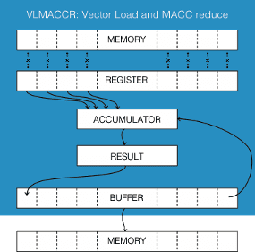
Thirdly, the VPU implements instructions that would be characteristic of a VLIW accelerator. A good example of such an instruction is VLMACCR, illustrated in the figure below. This instruction first computes the dot product between a vector in a register and one loaded from memory. Then the dot product is accumulated onto the last element of the result register, and the elements of the result register then shifted, essentially like a ring buffer.

Finally, as a benefit of having the VPU closely integrated with the ALU, most vector instructions are encoded on only 16 bits and can be dual-issued with scalar arithmetic or the special IO instructions offered by the xcore architecture. This means that, for instance, while the VPU is computing a dot product, pointer arithmetic can be performed in parallel.
The four ideas above enable the implementations of typical linear algebra routines to consist of long sequences of uninterrupted VLMACCR instructions, yielding high arithmetic density. The code snippet below shows the inner loop of a convolution kernel with 16 output channels and 1×1 kernel size. This kernel implements a data-stationary convolution strategy, meaning that K corresponds to a location in the weight tensor while a vector of input data is held in a register. The inner loop of such kernels corresponds to a full rotation of the hardware ring buffer implemented by VLMACCR. Also, notice the pointer arithmetic issued simultaneously with the vector operations.
{sub K, K, OUT_CHAN_STRIDE;   vlmaccr K[0]};
{sub K, K, OUT_CHAN_STRIDE;   vlmaccr K[0]};
{sub K, K, OUT_CHAN_STRIDE;   vlmaccr K[0]};
{sub K, K, OUT_CHAN_STRIDE;   vlmaccr K[0]};
{sub K, K, OUT_CHAN_STRIDE;   vlmaccr K[0]};
{sub K, K, OUT_CHAN_STRIDE;   vlmaccr K[0]};
{sub K, K, OUT_CHAN_STRIDE;   vlmaccr K[0]};
{sub K, K, OUT_CHAN_STRIDE;   vlmaccr K[0]};
{sub K, K, OUT_CHAN_STRIDE;   vlmaccr K[0]};
{sub K, K, OUT_CHAN_STRIDE;   vlmaccr K[0]};
{sub K, K, OUT_CHAN_STRIDE;   vlmaccr K[0]};
{sub K, K, OUT_CHAN_STRIDE;   vlmaccr K[0]};
{sub K, K, OUT_CHAN_STRIDE;   vlmaccr K[0]};
{sub K, K, OUT_CHAN_STRIDE;   vlmaccr K[0]};
{sub K, K, OUT_CHAN_STRIDE;   vlmaccr K[0]};
{add K, K, CIG_STRIDE;        vlmaccr K[0]}
Driving a proprietary architecture to success requires a wide range of easy-to-use libraries and tools. The xcore.ai platform was designed to be compatible with software written for our previous generation of architecture, hence inheriting a rich set of libraries for IO tasks. For ease of custom application development, our team ported FreeRTOS to xcore.ai. The final piece of the puzzle is our neural network deployment toolchain, which we demonstrated in the recent tinyML Talks webcast. In the second part of this post, we will get into detail how the deployment tools work, and how their ease of use can reduce time to market and development costs.


